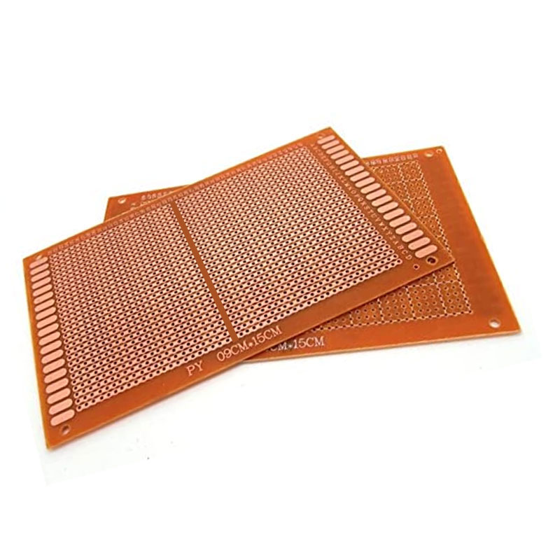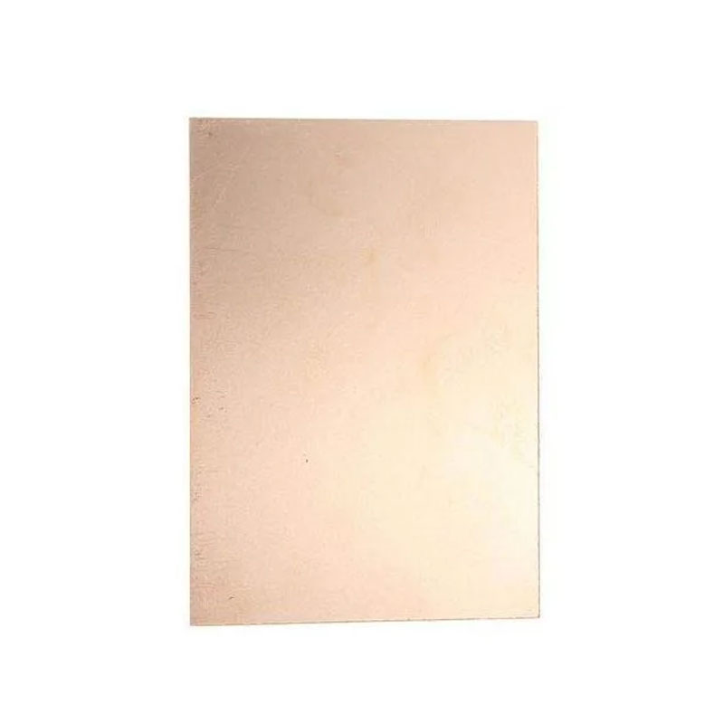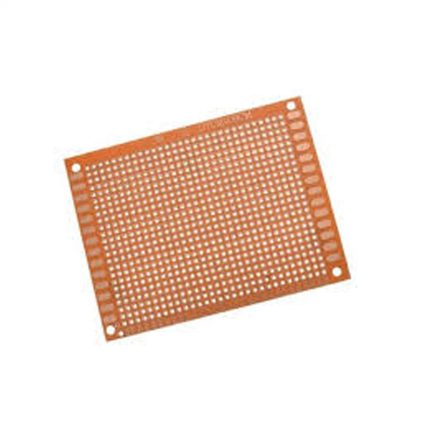
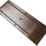

PCB board Line FR2 7X9 cm2
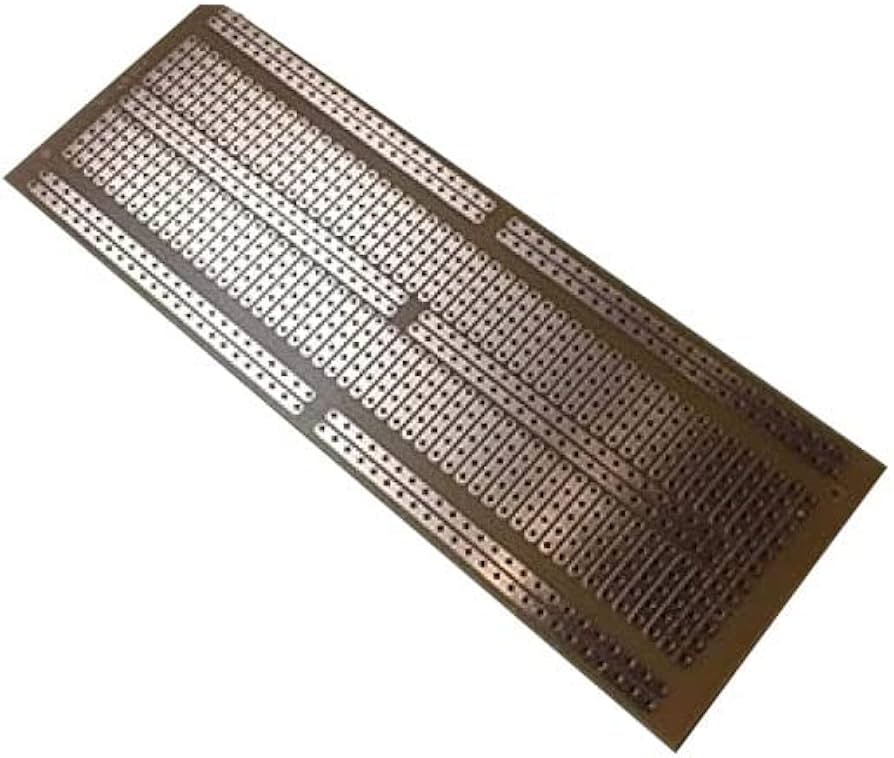
- 🟤 FR2 PCB prototyping board (stripboard / line board)
- 📏 Size: 7 × 9 cm for compact DIY circuits
- 🔩 Copper strip tracks for quick soldering without etching
- 🛠️ Easy to cut tracks to create custom connections
- 🧩 Ideal for prototypes, repairs, and small electronics projects
- 📦 FR2 phenolic material—lightweight and cost-effective
- 🔌 Works great with through-hole components
- ✅ Perfect for Arduino modules and general circuit building
20,00 EGP
In stock
In stock
Payment Methods:
Description
A FR2 PCB (Printed Circuit Board) of size 7×9 cm² is a type of fiberglass-reinforced board commonly used in electronics for creating circuits. FR2 is an older and more affordable material used in PCB fabrication, which is primarily made from phenolic resin and fiberglass. It’s used in many low-cost and basic electronic applications, especially for small-scale or prototype designs.
Key Details for FR2 PCB Board (7×9 cm²):
1. Material:
- FR2 (Phenolic Resin): The FR2 PCB material is composed of phenolic resin and fiberglass, making it less expensive than more advanced PCB materials like FR4. However, it is more brittle and less durable compared to FR4.
- Thickness: The typical thickness for FR2 boards ranges from 1.0 mm to 1.6 mm, but it can vary depending on the manufacturer and your specific needs.
2. Size:
- Dimensions: 7 cm x 9 cm (or 70 mm x 90 mm) is the size of the PCB. This is a relatively small, standard size for prototype boards, commonly used in hobby electronics or small devices.
- Area: 63 cm² total area (7 cm x 9 cm).
3. Copper Cladding:
- FR2 boards are typically copper-clad, meaning they come with a thin layer of copper foil on one or both sides. The copper layer allows the creation of circuits by etching away parts of it to create conductive paths for electrical signals.
- Copper thickness is usually 35 µm (1 oz/ft²), but it can vary depending on the board’s specifications.
4. Applications:
- Prototype Circuits: FR2 is often used for low-cost prototype boards in hobby projects and experimental designs.
- Low-power Electronics: Since FR2 is more fragile and less heat-resistant than FR4, it is typically used for circuits that operate at lower power.
- Toys and Consumer Electronics: FR2 is often found in lower-end consumer electronics or simple devices that don’t require robust performance or high durability.
5. Mechanical Properties:
- Brittleness: FR2 has a lower mechanical strength compared to FR4, making it more prone to cracking or breaking if handled roughly.
- Heat Resistance: FR2 is less heat-resistant than FR4. While FR2 boards can handle some heat, they may warp or degrade at temperatures above 130–140°C, which limits its usage in high-temperature environments.
6. Etching Process:
- The process of creating the circuit on an FR2 PCB typically involves the following steps:
- Design: The schematic is designed in PCB design software.
- Printing: The design is printed onto the board (usually with a toner transfer method or direct UV exposure).
- Etching: The copper areas not protected by the printed design are etched away using an etchant (e.g., ferric chloride or ammonium persulfate).
- Drilling: Holes are drilled for component leads (if needed).
- Soldering: After the etching process, the components are soldered onto the board.
7. Cost and Availability:
- Cost-Effective: FR2 PCBs are generally cheaper than FR4 PCBs and are readily available from electronics suppliers. They are ideal for prototyping or simple, low-budget projects.
- Standardization: You can purchase FR2 boards in standard sizes (such as 7×9 cm²) or larger sheets that you can cut to your desired dimensions.
Example: Using FR2 PCB (7×9 cm²) in a Simple Project
Components Required:
- FR2 PCB (7×9 cm²) board
- Soldering iron and solder wire
- Copper-clad FR2 PCB
- Etching solution (Ferric Chloride or Ammonium Persulfate)
- Electronic components (resistors, capacitors, ICs, etc.)
- Drill for making holes (if needed)
- PCB Design Software (like KiCad or Eagle)
Simple Process for Creating a Circuit:
-
Designing the Circuit: Using software like KiCad or Eagle, design your circuit and export the Gerber files or PCB layout.
-
Printing the Design: If you’re using the toner transfer method, print the design on glossy paper (or directly onto the PCB if using a direct UV method).
-
Transferring the Design: If using the toner transfer method, place the printed design against the PCB, heat it up, and transfer the design onto the copper surface using an iron.
-
Etching the Board: Use an etching solution (such as ferric chloride) to etch away the unwanted copper, leaving only the traces for your circuit.
-
Drilling: Drill holes for component leads if necessary.
-
Soldering: Place the components on the board and solder them in place.
-
Testing the Circuit: Once the circuit is complete, test it to ensure it functions as intended.
Advantages and Disadvantages of FR2 PCB (7×9 cm²):
Advantages:
- Low Cost: FR2 boards are affordable, which is ideal for hobbyists, students, and those working on simple projects or prototypes.
- Availability: Easy to find in most electronics stores or online platforms.
- Simple Prototyping: Suitable for creating simple, low-power circuits and rapid prototyping.
Disadvantages:
- Fragility: FR2 is more brittle compared to FR4, and the board can break or crack easily, especially when handled roughly.
- Limited Heat Resistance: Not suitable for high-temperature applications. It can start to degrade at temperatures above 130–140°C.
- Lower Durability: Less durable in the long term, especially in environments with higher temperatures or mechanical stress.
Specification
General
| WeightWeight | 0,00 g |
|---|---|
| Product Name | PCB Board – FR2 7×9 cm² |
| Type | Single-Sided PCB Board |
| Material | FR2 (Phenolic Paper) |
| Copper Layer | Single-Sided |
| Board Dimensions | 70×90 mm (7×9 cm²) |
| Thickness | 1.6 mm (typical) |
| Color | Brown |
| Surface Finish | Untinned / Raw Copper |
| Operating Temperature | -40°C to +105°C |
| Applications | DIY Electronics, Prototyping, Circuit Fabrication, Arduino Projects |
| Package Contents | 1× PCB Board – FR2 7×9 cm² |