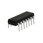
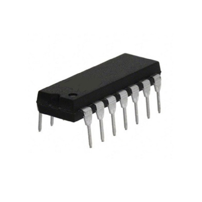
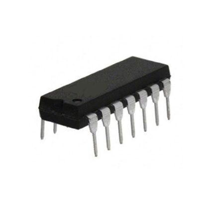
7486 Quad EXCLUSIVE-OR Gate
- Contains four independent 2-input XOR gates
- Operates on standard TTL logic levels
- Used for parity checking, bitwise addition, and logic functions
- Fast switching speed with low power consumption
- Widely used in digital circuits and signal processing
14,00 EGP
In stock
In stock
17
People watching this product now!
Payment Methods:
Description
Features
Compares 4-bit Binary or BCD Codes and Outputs Greater, Less Than or Equal
Outputs Directly Interface to CMOS, NMOS and TTL
Large Operating Voltage Range
Wide Operating Conditions
Pin Layout
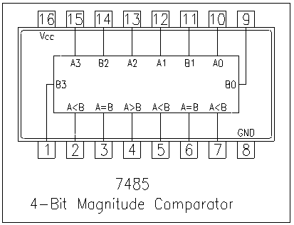
Pin Description
| Pin Number | Description |
|---|---|
| 1 | B3 Input |
| 2 | A |
| 3 | A=B Input |
| 4 | A>B Input |
| 5 | A>B Output |
| 6 | A=B Output |
| 7 | A |
| 8 | Ground |
| 9 | B0 Input |
| 10 | A0 Input |
| 11 | B1 Input |
| 12 | A1 Input |
| 13 | A2 Input |
| 14 | B2 Input |
| 15 | A3 Input |
| 16 | Vcc – Positive Supply |
Dimensional Drawing

Technical Data
Absolute Maximum Ratings
|
Supply Voltage |
7V |
|
Input Voltage |
5.5V |
|
Operating Free Air Temperature |
0°C to +70°C |
|
Storage Temperature Range |
-65°C to +150°C |
Recommended Operating Conditions
| Symbol | Parameter | Min | Typ | Max | Units |
|---|---|---|---|---|---|
| Vcc | Supply Voltage | 4.75 | 5 | 5.25 | V |
| Vih | HIGH Level Input Voltage | 2 | V | ||
| Vil | LOW Level Input Voltage | 0.8 | V | ||
| Ioh | HIGH Level Output Current | -0.4 | mA | ||
| Iol | LOW Level Output Current | 16 | mA | ||
| Ta | Free Air Operating Temperature | 0 | 70 | °C |
Electrical Characteristics
| Symbol | Parameter | Conditions | Min | Typ | Max | Units |
|---|---|---|---|---|---|---|
| Vi | Input Clamp Voltage | Vcc=Min Ii=-12mA | -1.5 | V | ||
| Voh | HIGH Level Output Voltage | Vcc=Min Ioh=MAX Vil=MAX | 2.4 | 3.4 | V | |
| Vol | LOW Level Output Voltage | Vcc=Min Iol=MAX Vih=MAX | 0.2 | 0.4 | V | |
| Ii | Input Current@MAX Input Voltage | Vcc=Max Vi=5.5V | 1 | mA | ||
| Iih | HIGH Level Input Current | Vcc=Max Vi=2.4V | 40 | µA | ||
| Iil | LOW Level Input Current | Vcc=Max Vi=0.4V | -1.6 | mA | ||
| Ios | Short Circuit Output Current | Vcc=Max | -18 | -55 | mA | |
| Icch | Supply Current with Outputs HIGH | Vcc=Max | 4 | 8 | mA | |
| Iccl | Supply Current with Outputs LOW | Vcc=Max | 12 | 22 | mA |
Switching Characteristics at Vcc=5V,Ta=25°C
| Symbol | Parameter | Conditions | Min | Typ | Max | Units |
|---|---|---|---|---|---|---|
| tplh | Propagation Delay Time LOW-to-HIGH Level Output | Cl=15pF Rl=400R | 22 | nS | ||
| tphl | Propagation Delay Time HIGH-to-LOW Level Output | Cl=15pF Rl=400R | 15 | nS |
Specification
General
| WeightWeight | 0,0000 g |
|---|---|
| function | Implements the EXCLUSIVE-OR (XOR) logic function with four independent XOR gates. |
| logic-operation | Output is high (1) if an odd number of inputs are high. For inputs A and B, 𝐴⊕𝐵 A⊕B is true if either A or B is true, but not both. |
| inputs | Four XOR gates, each with two inputs (A and B). |
| outputs | Four outputs, one for each XOR gate. |
| power-supply | Operates at 4.75V to 5.25V (standard 5V TTL logic). |
| current | Input Current: Low (typically a few microamperes). Output Drive Current: Up to 8 mA. |
| propagation-delay | Approximately 8-15 ns. |
| temperature-range | 0°C to 70°C (commercial grade) or -40°C to 85°C (industrial grade). |
| package-types | DIP-14, SOIC-14, TSSOP-14, and other surface-mount packages. |


