
 - Ekostra Electronics In Egypt اكوسترا الكترونيكس")
[match_prediction match_id="3"]
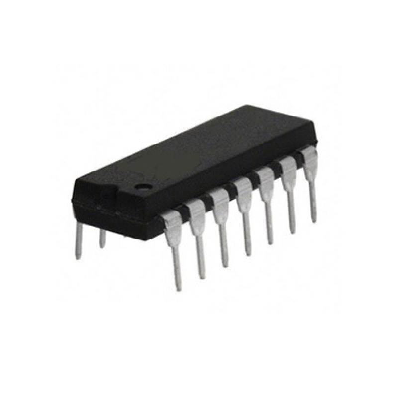
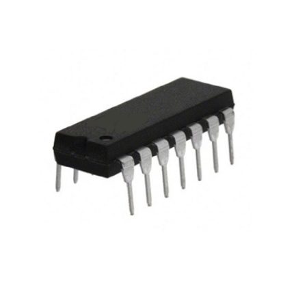
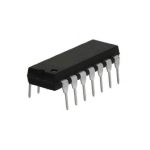
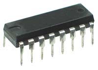
7447 BCD to 7-segment Decoder/Driver (Open Collector)
- Converts 4-bit BCD input to 7-segment display output
- Drives common-anode 7-segment displays
- Open-collector outputs for direct LED control
- Supports standard TTL logic levels
- Widely used in digital counters, clocks, and display systems
25,00 EGP
14
People watching this product now!
Description
7447 BCD to 7-Segment Decoder/Driver Datasheet
Photograph
Features
- Single BCD to 7-Segment Decoder with Open Collector Output
- Outputs Directly Interface to CMOS, NMOS and TTL
- Large Operating Voltage Range
- Wide Operating Conditions
Pin Layout

Pin Description
| Pin Number | Description |
|---|---|
| 1 | BCD B Input |
| 2 | BCD C Input |
| 3 | Lamp Test |
| 4 | RB Output |
| 5 | RB Input |
| 6 | BCD D Input |
| 7 | BCD A Input |
| 8 | Ground |
| 9 | 7-Segment e Output |
| 10 | 7-Segment d Output |
| 11 | 7-Segment c Output |
| 12 | 7-Segment b Output |
| 13 | 7-Segment a Output |
| 14 | 7-Segment g Output |
| 15 | 7-Segment f Output |
| 16 | Vcc – Positive Supply |
Dimensional Drawing

Technical Data
Absolute Maximum Ratings
|
Supply Voltage |
7V |
|
Input Voltage |
5.5V |
|
Operating Free Air Temperature |
0°C to +70°C |
|
Storage Temperature Range |
-65°C to +150°C |
Recommended Operating Conditions
| Symbol | Parameter | Min | Typ | Max | Units |
|---|---|---|---|---|---|
| Vcc | Supply Voltage | 4.75 | 5 | 5.25 | V |
| Vih | HIGH Level Input Voltage | 2 | V | ||
| Vil | LOW Level Input Voltage | 0.8 | V | ||
| Ioh | HIGH Level Output Current | -0.4 | mA | ||
| Iol | LOW Level Output Current | 16 | mA | ||
| Ta | Free Air Operating Temperature | 0 | 70 | °C |
Electrical Characteristics
| Symbol | Parameter | Conditions | Min | Typ | Max | Units |
|---|---|---|---|---|---|---|
| Vi | Input Clamp Voltage | Vcc=Min Ii=-12mA | -1.5 | V | ||
| Voh | HIGH Level Output Voltage | Vcc=Min Ioh=MAX Vil=MAX | 2.4 | 3.4 | V | |
| Vol | LOW Level Output Voltage | Vcc=Min Iol=MAX Vih=MAX | 0.2 | 0.4 | V | |
| Ii | Input Current@MAX Input Voltage | Vcc=Max Vi=5.5V | 1 | mA | ||
| Iih | HIGH Level Input Current | Vcc=Max Vi=2.4V | 40 | µA | ||
| Iil | LOW Level Input Current | Vcc=Max Vi=0.4V | -1.6 | mA | ||
| Ios | Short Circuit Output Current | Vcc=Max | -18 | -55 | mA | |
| Icch | Supply Current with Outputs HIGH | Vcc=Max | 4 | 8 | mA | |
| Iccl | Supply Current with Outputs LOW | Vcc=Max | 12 | 22 | mA |
Switching Characteristics at Vcc=5V,Ta=25°C
| Symbol | Parameter | Conditions | Min | Typ | Max | Units |
|---|---|---|---|---|---|---|
| tplh | Propagation Delay Time LOW-to-HIGH Level Output | Cl=15pF Rl=400R | 22 | nS | ||
| tphl | Propagation Delay Time HIGH-to-LOW Level Output | Cl=15pF Rl=400R | 15 | nS |
هذا الوصف والمواصفات تمت كتابته بمساعدة الذكاء الاصطناعي، يُرجى مراجعته قبل الشراء.
برجاء تأكيد الطلب على
الواتساب
للتأكد من توفر المخزون قبل الدفع
Specification
General
| WeightWeight | 0,0000 g |
|---|---|
| package-types | Package Types: |
| function | Converts 4-bit BCD input to 7-segment display output. |
| inputs | BCD Inputs: 4-bit binary inputs (A, B, C, D) to represent decimal digits (0-9). Enable Inputs: LE (Latch Enable): Latches the BCD input data into the internal register when enabled. BI (Blanking Input): Blanks the display if active (low level). LT (Lamp Test): Turns on all segments for testing if active (low level). |
| outputs | Seven Segments (a-g): Open-collector outputs connected to the segments of the 7-segment display. Blanking and Lamp Test: Control and test the display. |
| operating-voltage | Typically operates between 4.75V to 5.25V. |
| current | Output Drive Current: Can source/sink typically up to 25 mA per segment. Input Current: Low input current for digital inputs. |
| open-collector | Requires external pull-up resistors. |
| temperature-range | Typically operates within 0°C to 70°C or -40°C to 85°C for industrial-grade versions. |