
7432 Quad 2-Input OR Gate Datasheet
- Contains four independent 2-input OR gates
- Operates at standard 5V TTL logic levels
- Fast switching with low propagation delay
- Low power consumption
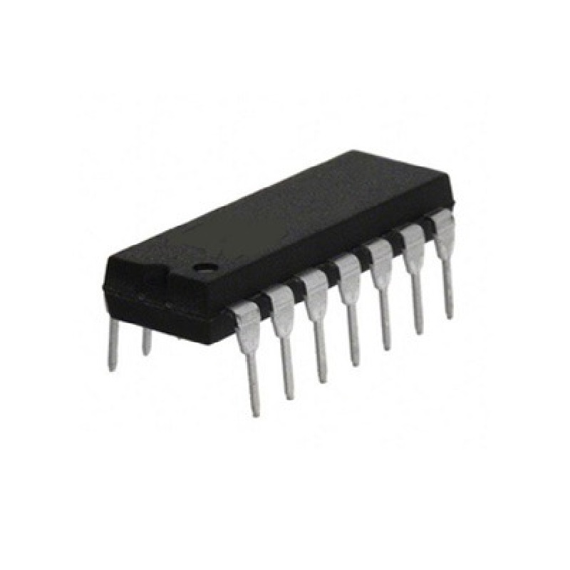
- Comes in 14-pin DIP or SMD packages
14,00 EGP
13
People watching this product now!
Payment Methods:
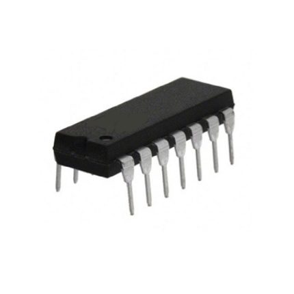
Description
Photograph

Features
- Four 2-Input Logic OR Gates
- Outputs Directly Interface to CMOS, NMOS and TTL
- Large Operating Voltage Range
- Wide Operating Conditions
Pin Layout

Pin Description
| Pin Number | Description |
|---|---|
| 1 | A Input Gate 1 |
| 2 | B Input Gate 1 |
| 3 | Y Output Gate 1 |
| 4 | A Input Gate 2 |
| 5 | B Input Gate 2 |
| 6 | Y Output Gate 2 |
| 7 | Ground |
| 8 | Y Output Gate 3 |
| 9 | A Input Gate 3 |
| 10 | B Input Gate 3 |
| 11 | Y Output Gate 4 |
| 12 | A Input Gate 4 |
| 13 | B Input Gate 4 |
| 14 | Vcc – Positive Supply |
Dimensional Drawing

Technical Data
Absolute Maximum Ratings
|
Supply Voltage |
7V |
|
Input Voltage |
5.5V |
|
Operating Free Air Temperature |
0°C to +70°C |
|
Storage Temperature Range |
-65°C to +150°C |
Recommended Operating Conditions
| Symbol | Parameter | Min | Typ | Max | Units |
|---|---|---|---|---|---|
| Vcc | Supply Voltage | 4.75 | 5 | 5.25 | V |
| Vih | HIGH Level Input Voltage | 2 | V | ||
| Vil | LOW Level Input Voltage | 0.8 | V | ||
| Ioh | HIGH Level Output Current | -0.4 | mA | ||
| Iol | LOW Level Output Current | 16 | mA | ||
| Ta | Free Air Operating Temperature | 0 | 70 | °C |
Electrical Characteristics
| Symbol | Parameter | Conditions | Min | Typ | Max | Units |
|---|---|---|---|---|---|---|
| Vi | Input Clamp Voltage | Vcc=Min Ii=-12mA | -1.5 | V | ||
| Voh | HIGH Level Output Voltage | Vcc=Min Ioh=MAX Vil=MAX | 2.4 | 3.4 | V | |
| Vol | LOW Level Output Voltage | Vcc=Min Iol=MAX Vih=MAX | 0.2 | 0.4 | V | |
| Ii | Input Current@MAX Input Voltage | Vcc=Max Vi=5.5V | 1 | mA | ||
| Iih | HIGH Level Input Current | Vcc=Max Vi=2.4V | 40 | µA | ||
| Iil | LOW Level Input Current | Vcc=Max Vi=0.4V | -1.6 | mA | ||
| Ios | Short Circuit Output Current | Vcc=Max | -18 | -55 | mA | |
| Icch | Supply Current with Outputs HIGH | Vcc=Max | 4 | 8 | mA | |
| Iccl | Supply Current with Outputs LOW | Vcc=Max | 12 | 22 | mA |
Switching Characteristics at Vcc=5V,Ta=25°C
| Symbol | Parameter | Conditions | Min | Typ | Max | Units |
|---|---|---|---|---|---|---|
| tplh | Propagation Delay Time LOW-to-HIGH Level Output | Cl=15pF Rl=400R | 22 | nS | ||
| tphl | Propagation Delay Time HIGH-to-LOW Level Output | Cl=15pF Rl=400R | 15 | nS |
Specification
General
| WeightWeight | 0,0000 g |
|---|---|
| logic-family | TTL (Transistor-Transistor Logic) |
| number-of-gates | 4 |
| number-of-inputs-per-gate | 2 |
| output-type | Standard TTL (Push-Pull) |
| supply-voltage-vcc | Typically 5V |
| input-voltage-range | 0V to 5V (compatible with TTL levels) |
| output-voltage-high-voh | Typically 2.7V (when Vcc = 5V) |
| output-voltage-low-vol | Typically 0.4V (when Vcc = 5V) |
| propagation-delay | Approximately 10-15 ns (varies with the manufacturer and conditions) |
| power-dissipation | Typically 1W (varies with load and supply voltage) |
| package-types | 14-pin Dual In-Line Package (DIP) |
Customer Reviews
Related Products


-20%
Original price was: 150,00 EGP.120,00 EGPCurrent price is: 120,00 EGP.